THIS ARTICLE/PRESS RELEASE IS PAID FOR AND PRESENTED BY NTNU Norwegian University of Science and Technology - read more
Researchers can now see how individual atoms arrange themselves in materials
Atomic-level 3D models can teach us more about why electronic gadgets work.
Although nanotechnology and materials science are complicated topics for most of us, the research in these fields is of great importance to almost everyone. Your digital gadgets, for example, are completely dependent on it.
Today, all microelectronics depend on semiconductors. These are materials that are not very good at conducting electricity. But you can add tiny amounts of other substances to them, a process known as 'doping'. This improves the semiconductor’s performance so they’re not so bad after all.
“In the past, we doped semiconductors and saw that this drastically changed the electrical properties of the material,” says PhD candidate Kasper Aas Hunnestad at NTNU’s Department of Materials Science and Engineering.
This is all well and good. It’s nice when something works. But beyond the fact that it works, we haven’t always understood very much of why it does. This is especially true at the atomic level.
"Now we know more about how we can measure the individual added atoms and why they work. These atoms are very difficult to find," Hunnestad says.

Why ‘knowing why’ is important
Why should we care about single atoms and why something works? Isn’t it good enough just to know that it does?
“Only when you know more about how something works, can you manipulate the material and optimise it,” Dennis Meier says. He is a professor in the Department of Materials Science and Engineering at NTNU, who led the project.
This way, for example, you can make more efficient, environmentally friendly, or cheaper materials for the job to be done. Or you can assign new properties to a material that you already have available with much greater precision. This is also key for developing future materials for sustainable technology.
“Often, we want to introduce new functionality to materials. For that we need to know exactly what role each individual atom plays,” says Meier.
Advanced imaging techniques make it possible
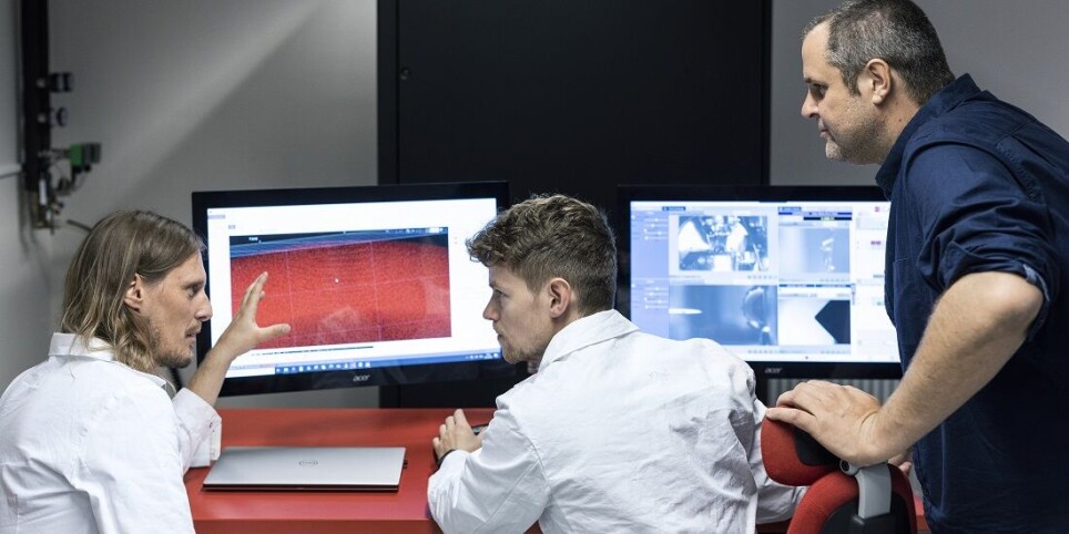
Hunnestad and colleagues present the results of many, many hours of work using 'atom probe tomography' (APT) in a recent article in Nature Communications.
APT is an advanced piece of cutting-edge equipment that NTNU acquired a few years ago. The machine can provide a three-dimensional representation of what a material looks like, right down to the atomic level, explains Constantinos Hatzoglou. He is a senior engineer in the APT laboratory at the Department of Materials Science and Engineering.
Hunnestad and colleagues utilised this outstanding capability to study a new type of oxide-based semiconductor to which very small amounts of a substance have been added to tailor its properties.
“Conventional microscopy techniques didn’t allow us to observe how small amounts of additives positioned themselves in semiconductors,” Hunnestad says.
Shows the enormous potential
Hunnestad and Professor Meier agree on the great potential APT has for their research. They believe the APT machine makes ground-breaking research possible.
They are enthusiastic about all the fascinating possibilities that have already emerged from their APT-based research and the novel perspectives for the characterization of functional materials at the atomic scale.
Hunnestad has worked with APT for about three years. He has carried out extensive correlated microscopy measurements, supported by Antonius van Helvoort and Per Erik Vullum. Van Helvoord is a professor at NTNU’s Department of Physics and experts in high-resolution electron microscopy, while Vullum is a professor II at NTNU, Department of Physics and senior researcher at SINTEF Industry.
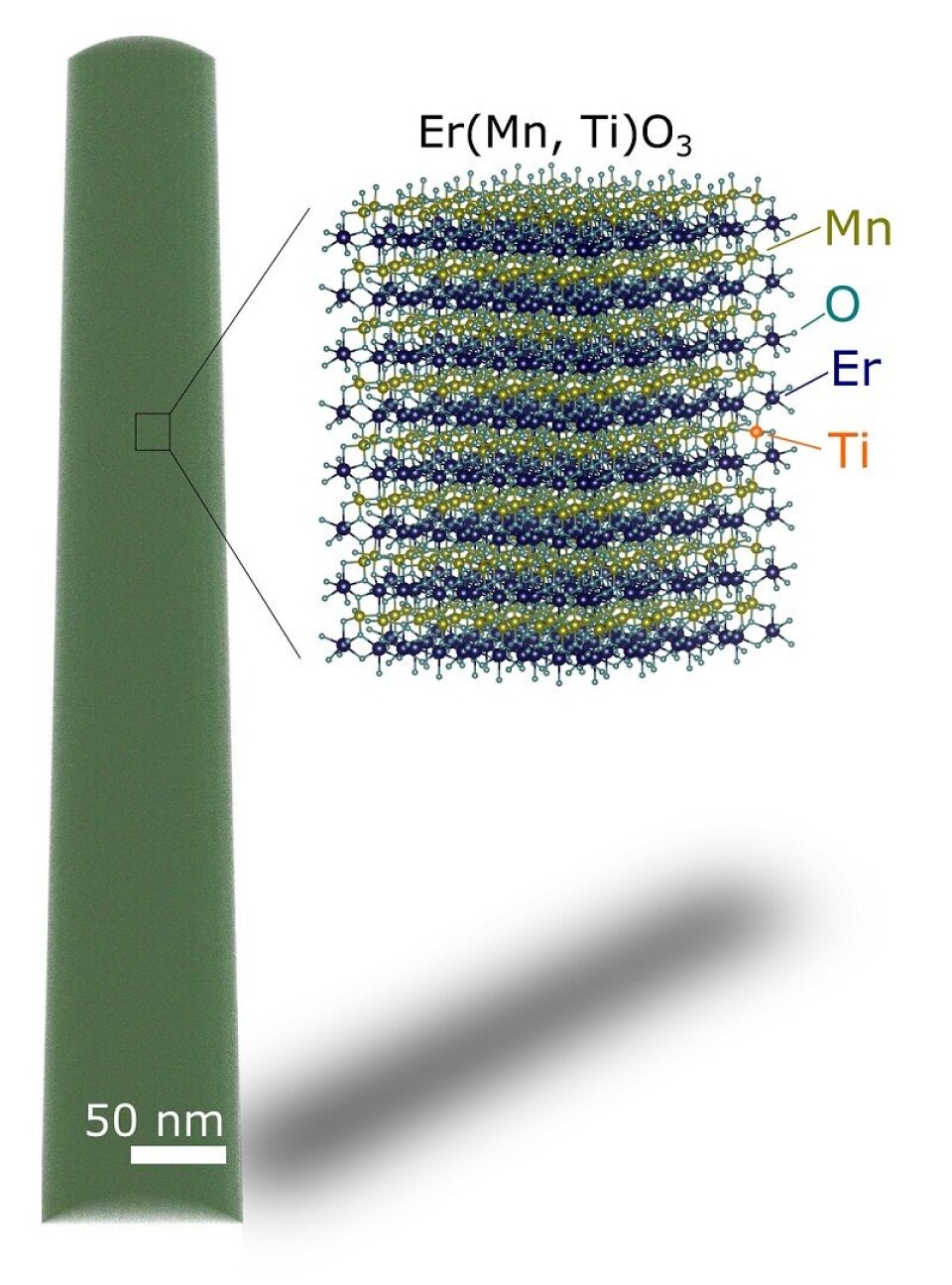
Imaging of individual titanium atoms mixed into a semiconductor
The research group looked at the oxide-based semiconductor Er(Mn,Ti)O3. For this purpose, their collaborators at the Lawrence Berkeley National Laboratory in the USA added tiny amounts of the element titanium (Ti) to erbium manganate (ErMnO3).
“With the atom probe, we can get a three-dimensional representation of how the titanium atoms are positioned in the semiconductor,” says Meier. “This allows us to link the new electrical properties of the material all the way down to individual atoms.”
Dr. Muhammad Zeeshan Khalid is a member of the team headed by Sverre Selbach, a professor at NTNU’s Department of Materials Science and Engineering. He supplemented the experiments with calculations. These calculations provide further insight into the effects that individual atoms can have on the physical properties.
“The procedures and the results are of broad interest. They can extend our understanding of oxide-based semiconductors and functional materials in general. The research opens completely new doors,” Meier says.
Reference:
Hunnestad et al. Atomic-scale 3D imaging of individual dopant atoms in an oxide semiconductor. Nature Communications, 2022.

Read more content from NTNU:
-
Why some people can’t stop pulling out their hair or picking their skin
-
Can Europe create AI that we actually understand?
-
Doctors and nurses believe their own substance use affects patients
-
When the offshore wind turbines fall silent: What happens to the waste?
-
“Norway used German soldiers to clear minefields and dump explosives in fjords and lakes"
-
Physicists may have found the missing link for quantum computers


