This article was produced and financed by The Research Council of Norway

New material may replace silicon
A new method for producing semiconductors from graphene has been developed by Norwegian scientists. This finding may revolutionise the technology industry.
Denne artikkelen er over ti år gammel og kan inneholde utdatert informasjon.
This video explains the new material. (Video: CrayNano AS)
The method involves growing semiconductor-nanowires on graphene. To achieve this, researchers “bomb” the graphene surface with gallium atoms and arsenic molecules, thereby creating a network of minute nanowires.
The result is a one-micrometre thick hybrid material which acts as a semiconductor. By comparison, the silicon semiconductors in use today are several hundred times thicker. The semiconductors’ ability to conduct electricity may be affected by temperature, light or the addition of other atoms.
Fantastic potential
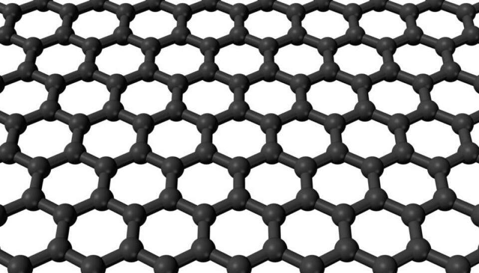
Graphene is the thinnest material known, and at the same time one of the strongest. It consists of a single layer of carbon atoms and is both pliable and transparent. The material conducts electricity and heat very effectively. And perhaps most importantly, it is very inexpensive to produce.
“Given that it’s possible to make semiconductors out of graphene instead of silicon, we can make semiconductor components that are both cheaper and more effective than the ones currently on the market,” explains Helge Weman of the Norwegian University of Science and Technology (NTNU). Weman is behind the breakthrough discovery along with Professor Bjørn-Ove Fimland.
“A material comprising a pliable base that is also transparent opens up a world of opportunities, one we have barely touched the surface of,” says Weman. “This may bring about a revolution in the production of solar cells and LED components. Windows in traditional houses could double as solar panels or a TV screen. Mobile phone screens could be wrapped around the wrist like a watch. In short, the potential is tremendous.”
Broad-based public funding
The researchers have received assistance in gaining patents and founding a company from NTNU Technology Transfer AS, a collaborative partner to the programme entitled Commercialising R&D Results (FORNY2020) at the Research Council of Norway.
However, the path to these remarkable findings started with basic research funded under the Research Council’s Clean Energy for the Future Programme (RENERGI) and the now-concluded programme, Nanotechnology and New Materials (NANOMAT), which initiated the findings.
Huge interest among electronics giants
The researchers will now begin to create prototypes directed towards specific areas of application. They have been in contact with giants in the electronics industry such as Samsung and IBM. “There is tremendous interest in producing semiconductors out of graphene, so it shouldn’t be difficult to find collaborative partners,” Weman adds.
The researchers are hoping to have the new semiconductor hybrid materials on the commercial market in roughly five years.
Translated by: Glenn Wells/Carol B. Eckman


