An article from Norwegian SciTech News at SINTEF

Nano-level detective
Scientists have created an X-ray detector that can reveal the composition of materials in a fraction of a second.
Denne artikkelen er over ti år gammel og kan inneholde utdatert informasjon.
The sensor has been developed by nanotechnologists from Norwegian research institution SINTEF and is already an exclusive component in great demand by industries that supply advanced analytical instruments for materials science.
This type of sensor is known as a silicon drift diode (SDD), and it is the basic component of a number of instruments that are used in everything from medical X-ray systems to monitoring experiments at CERN, the European Organization for Nuclear Research, where scientists are searching for the most basic building blocks of matter.
Another application is in art and archaeology, where the detector can identify which materials have been used and just what they consist of.
One grain of dust can destroy
The sensor consists of a double-sided microstructure which is fabricated on silican wafers. Such structures are complex, and difficult to produce.
"Today, we are one of only two or three suppliers of such sensors in the whole world,” says research SINTEF scientist Niaz Ahmed.
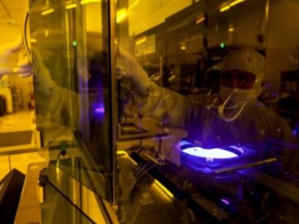
Although the tiny device measures no more than 8 x 8 millimetres, it takes eight weeks to produce, and the entire fabrication needs to take place in a super-clean environment.
A single grain of dust is capable of destroying the whole process by short-circuiting the equipment, or damaging its nano-scale structures.
That is why the advanced laboratory is equipped with vibration-reducing foundations and air-filtration systems that remove particles as small as 100 nanometres from the laboratory.
The sensor is produced by oxidising the silicon wafer in several stages, creating a physical structure on a nanometre scale. Once this has been done, the scientists dope it with charged atoms at various levels.
The result is an incredibly light-sensitive diode which, once it has been connected to the appropriate electronics, can reveal changes in the physical structure of most materials.
Calculating energy
The sensor uses spectroscopy, which is based on sending light through a transparent object. When the light beam emerges from the other side of the object, the sensor reads off changes in its characteristics.
“To put it simply, we can say that the sensor sorts the light into its individual energy levels by counting the photons and calculating their energy,” says Ahmed.
Unlike standard silicon-based sensors, the way the SDDs work requires them to have structures on both surfaces of the sensor chip.
“This can only be done with the help of advanced equipment and extremely high levels of accuracy,” says the SINTEF scientist, and explains how.
One side of the sensor is called the “window side”, and is turned towards the source of radiation. It absorbs the X-ray beam almost without loss.
The other side is known as the “ring side” and has a concentric annular structure; i.e. the rings have the same centre but increase in radius, something like a parabolic aerial in microformat. This means that the electrons generated by the radiation source are captured by the central electrode, which in turn enables the X-ray sensor to discard all the irrelevant electronic signals, or “noise”.
Because it easily distinguishes between different materials by registering differences in the absorption energy of their component elements, the chip can be used to identity forbidden materials such as lead, cadmium and mercury.
Due to its unique sensitivity, the sensor is in very high demand, not only in Norway where it is developed, but in the world market as well. The researchers have also managed to make it so efficient that it uses very little energy, which is important when the sensor is connected to other electronics.