This article was produced and financed by The Research Council of Norway

Potential to replace silicon
Smaller, cheaper, better products when you combine graphene and semiconductor technology .
Denne artikkelen er over ti år gammel og kan inneholde utdatert informasjon.
Mobile phones that bend, self-powered nanodevices, new and improved solar cell technology and windows that generate electricity are but a few of the potential products from the union of semiconductors and graphene.
Semiconductors grown on graphene at the Norwegian University of Science and Technology (NTNU) may be the most important research breakthrough of 2012 in Norway. At the centre of the research efforts are Professor Helge Weman, Professor Bjørn-Ove Fimland and post-doctoral fellow Dong-Chul Kim.
The team is now working on translating the results of their basic research into an initial prototype.
Just one atom thick
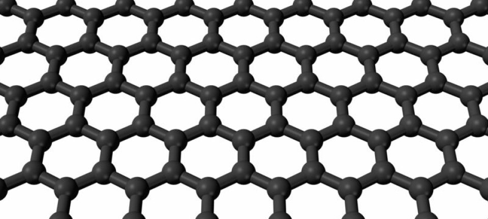
In the 1960s, researchers envisioned that graphite (pure carbon) could be cut into layers measuring only one atom in thickness – resulting in the material known as graphene.
In the 1990s, researchers managed to create a layer as thin as 100 atoms, but there was no progress after that until 2004, when Russian-born Andre Geim grabbed a tape dispenser from his desk at the University of Manchester, pressed a bit of tape over a thin layer of graphite and peeled it away. When he examined the tape under a microscope, he discovered a layer only one carbon atom thick. Graphene was born!
In 2010, Geim and his colleague, Konstantin Novoselov, were jointly awarded the Nobel Prize in Physics for their work in demonstrating the unique properties of graphene.
Ahead of the pack at NTNU
Six months before Geim and Novoselov arrived in Stockholm to receive their prize, and before graphene had become an item of interest, South Korean post-doctoral fellow Dong Chul Kim at NTNU had suggested to Professors Helge Weman and Bjørn-Ove Fimland at the Department of Electronics and Telecommunications that they should take a closer look at precisely this material.
The suggestion came shortly after the NTNU group already had succeeded in growing semiconductor nanowires made of gallium arsenide (GaAs) on silicon substrates. This led Weman to wonder if it would be possible to grow semiconductor nanowires directly on graphene instead.
The collective expertise of Weman, Fimland and Kim proved to be a fruitful combination. The researchers quickly achieved their first breakthrough of growing semiconductors nanowires on a one-atom-thick base in September 2010, and in the summer of 2012 they published their results in the American journal Nano Letters.
These active semiconductors normally grow to be one micron (a millionth of a metre) in thickness.
Will silicon become obsolete?
Graphene is definitely the hottest topic right now among nanomaterial researchers. The pure-carbon material is by far the thinnest and strongest known to exist. It is 200 times stronger than steel, conducts electricity 100 times faster than silicon and is superior to any other material in conducting heat. It is impermeable, yet pliable and transparent at the same time. And inexpensive large-scale production of graphene is now becoming a reality.
At present, electronics and solar cells are using thick silicon substrates. But silicon has clear limitations, including size. Large technology companies are struggling to produce silicon-based electronics that are smaller than those currently on the market.
Another challenge with using silicon is that silicon-based electronics generate a great deal of heat. Many people consider graphene to be the prime candidate for replacing silicon.
Large multinational corporations such as IBM and Samsung have poured a lot of effort into research on both semiconductors and graphene. But the real breakthrough in growing semiconductors on graphene actually took place at NTNU in Trondheim.
The findings of these researchers in Trondheim may be used to make electronics and solar cells that are several hundred times thinner than current models. This will make it possible to produce electronics that are both pliable and transparent, in addition to being less expensive and more energy-efficient.
More efficient solar cells and LEDs
It will probably not be long before simple graphene products begin appearing on the market. Some of them will be based on semiconductor technology.
Semiconductors are a main component in almost all modern electronics. Without them, it would not be possible to have computers, smartphones, solar cells, LED lights or devices using lasers, i.e. everything from printers to fibre communications. All these items can be made smaller and better using graphene. Graphene can both supplant the semiconductor substrate and serve as a transparent electrode for a pliable nanowire solar cell.
“Solar cell and LED technology will be the initial areas to see new products using semiconductors grown on graphene,” says Weman.
Under-priced fossil-fuel energy is the primary contributor to global warming. Sunlight is an alternative source with enormous potential, but solar energy will have to become less expensive and more efficient. Semiconductor nanowires based on graphene may just finally tip the scales in favour of solar energy.
“If semiconductor nanowires grown on graphene are used in solar cells, the same amount of sunlight can be converted to energy using one-tenth the volume of materials used in thin-film solar cells. And that means we’ve cut down on even more material by growing the semiconductors on graphene instead of on a thick semiconductor substrate. New research also shows that graphene has additional unique properties that enhance the efficiency of a solar cell,” Weman explains.
LED light bulbs are superior in terms of energy efficiency, but have been more expensive to produce because of costly semiconductor substrates. Semiconductor nanowires on graphene will make it possible to supply the world with LED lamps that are far cheaper and much more efficient while also being more pliable and weighing less than today’s lamps.
Industrialisation on the horizon
The work on graphene at NTNU has drawn the attention of many international companies interested in collaborating with the Trondheim-based researchers and their start-up company, CrayoNano. But the potential industrial queries so far have come solely from Asia and the US. Actors in Norway and Europe have yet to express any interest.
“We are pioneers in that we are using graphene for something other than basic research. We may already have our first prototype in place by the end of 2013, but we don’t wish to reveal what it is yet,” says Weman.
“The field we are working with – using graphene as a replacement for silicon and other semiconductor substrates in electronics and solar cells – entails many new opportunities. But the potential is just as great for applications using graphene in areas other than electronics, such as in the medical sector. Graphene can be used in the body without causing any harm,” explains Weman.
“In a world where drinking water is in short supply, employing oxygen-modified graphene filters to purify water is yet another exciting application. It’s a whole new way to turn seawater into fresh water.”
In any case, research and development activities will be needed for many years. Weman likens the current state of graphene research to where silicon was in the early 1960s.
A three-minute video on is available on YouTube in which Helge Weman explains this research.
Translated by: Glenn Wells/Darren McKellep


