An article from Norwegian SciTech News at SINTEF

New sensor protects astronauts against radiation
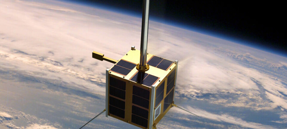
When NASA sets course for the International Space Station, Norwegian sensor technology will form part of the payload.
Denne artikkelen er over ti år gammel og kan inneholde utdatert informasjon.
While those of us who still have our feet on the ground are protected by the atmosphere, astronauts float around in a sphere that is quite unprotected against the lethal radiation of outer space.
This means that it is vital to monitor the many sources of radiation to which they are exposed, and just as important, the degree of exposure.
This is where a team of Norwegian scientists comes into the picture: they have developed a sensor, only a millimetre thick, that allows the source, type and strength of radiation to be measured, while simultaneously visualising the various parameters.
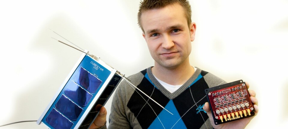
Both the sensor’s advanced functions and as its extremely small size have aroused the interest of NASA. The ISS needs to carry a great deal of equipment, and internal space is a critical factor, so, as sensor developer Niaz Ahmed of SINTEF’s Micro-and Nanotechnology laboratory (MiNaLab) in Oslo tells us, the sensor is soon to be ferried up to the ISS.
Advanced detective
Although the little device consists of a silicon wafer whose dimensions are only 1 x 17.5 x 17.5 mm, it contains no fewer than 256 x 256 active detector elements, each of them only 55 x 55 micrometres in size.
“A micrometre is one thousandth of a millimetre, or one two-hundredth part of the thickness of a hair, so these elements are invisible to the naked eye,” says Ahmed.
These tiny points are assembled in a matrix, and each element acts as a single pixel, which can “see” the radiation. The information is then processed by a tiny computer, with the result that the source, energy and type of radiation appear in the form of a three-dimensional image like a film.
The sensor is fabricated by oxidising the wafer in several stages to create a nanoscale physical structure. This done, the scientists add charged atoms to individual layers of the structure. The result is an incredibly light-sensitive diode which, once it is coupled to the appropriate electronics, can be used for x-ray imaging or to “see” other particles at atomic level.
Three sensitive months
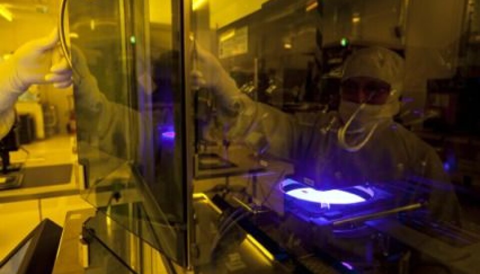
The fabrication process takes no less than 12 weeks, and is extremely sensitive: the merest mote of dust is capable of laying waste a whole production series by short-circuiting the equipment or destroying the microscopic nanoscale structures:
“Which is why our laboratory is vibration-proof and is equipped with air-filtration units that remove particles as small as 100 nanometres,” says the SINTEF scientist.
Second-generation x-ray equipment
The special technology on which the sensor is based is an advanced x-ray system which, unlike conventional x-ray equipment, is also capable of imaging soft tissue, thus enabling doctors and surgeons to visualise the internal organs of the body in three dimensions. Now, NASA has ordered a modified version of this technology for use in its own equipment.
The system as a whole will be manufactured by the University of Houston in Texas, although the sensor itself will be fabricated by MiNaLab in Oslo.
“So far, SINTEF is the only place in the world where these advanced components can be produced on such a small scale,” says Niaz Ahmed.
Since the sensor is etched on wafers that are 1 mm thick, it produces less noise than similar sensors that use wafers of only 0.3 mm.” The “noise” that Ahmed mentions consists of false signals that are a function of the characteristics of the sensor.
The sensor is also very exposed to high-energy radiation from space - radiation from which our atmosphere protects us.
Soon, the Norwegian sensor will be protecting NASA’s pioneers as they float around in space.


